AT A GLANCE
- Concept: Electrostatic Control: Wrapping the gate material completely around the channel maximizes the physical barrier against leakage.
- Concept: Short-Channel Effects: As transistors shrink below 3nm, standard architectures lose the physical ability to stop electron flow.
- Concept: Epitaxy: Foundries grow alternating layers of silicon and silicon-germanium atom by atom to create a superlattice.
- Concept: Selective Etching: Highly precise chemical gases dissolve the germanium without damaging the adjacent silicon nanosheets.
HOW IT WORKS
A transistor is a microscopic electrical switch. It consists of a channel that carries current and a gate that acts as an on/off valve. When the gate applies a voltage, electrons flow through the channel.
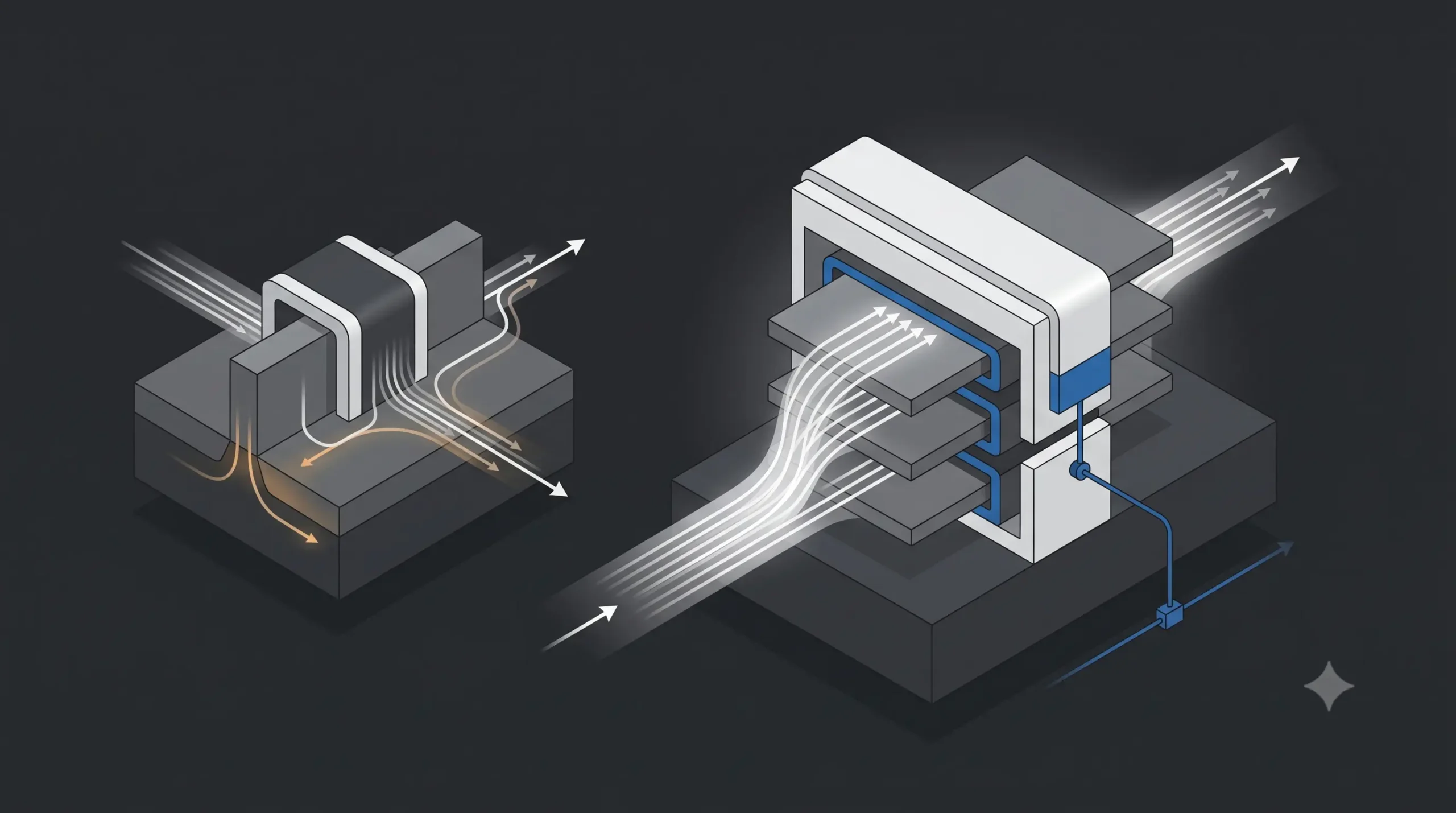
For the past decade, the semiconductor industry relied on the FinFET architecture. The channel stood up like a vertical fin, and the gate draped over three sides of it. This left the bottom of the fin physically exposed to the silicon substrate.
As foundries shrink transistor channels down to the 2-nanometer node, the distance between the source and the drain becomes so short that electrons begin jumping the gap even when the gate is turned off. Engineers call this subthreshold leakage. The exposed bottom of the FinFET becomes a massive vulnerability, bleeding power and generating extreme heat.
To stop this leakage, engineers transition to Gate-All-Around (GAA) nanosheets. They detach the channel from the substrate entirely. Instead of a vertical fin, the channel consists of multiple, ultra-thin, horizontal silicon ribbons stacked on top of each other.
The manufacturing process requires extreme chemical violence. Engineers first grow alternating layers of pure silicon and silicon-germanium. They then apply a highly selective isotropic etch. This specific chemical gas physically dissolves the silicon-germanium layers while ignoring the pure silicon.
The germanium vanishes, leaving the silicon ribbons suspended in mid-air. Foundries then use atomic layer deposition to pump organometallic vapors into these microscopic gaps. The vapor coats the suspended ribbons, building a high-k dielectric gate that perfectly wraps 360 degrees around every single nanosheet. This absolute physical enclosure restores complete electrostatic control over the electron flow.
Transistor Channel Electrostatic Control
Observe how Gate-All-Around (GAA) nanosheets prevent extreme subthreshold leakage at sub-5nm nodes compared to legacy architectures.
WHY IT MATTERS NOW
Artificial intelligence demands exponential increases in computational density and power efficiency. The thermal limits of data centers dictate the physical ceiling of AI capability. If leakage current is not stopped, a modern 100-billion transistor GPU will physically melt its own packaging.
GAA nanosheets represent the absolute bleeding edge of global industrial capacity. Intel brands this architecture “RibbonFET,” while Samsung achieved early volume production in late 2022. TSMC delayed its adoption to the N2 node, preferring the mature yields of FinFET for as long as physically possible.
Mastering this specific geometry separates tier-one semiconductor superpowers from the rest of the world. The transition from FinFET to GAA is not merely a design update; it forces foundries to completely overhaul their physical fabrication lines. It requires billions of dollars in new chemical vapor deposition tools and highly specialized etching equipment from suppliers like Applied Materials and Tokyo Electron.
The geopolitical consequences are absolute. A nation that successfully yields high-volume 2nm GAA logic chips controls the foundational hardware required to run next-generation autonomous weapons, hyper-scale intelligence models, and advanced cryptography. Those who fail the transition remain permanently locked in the FinFET era.
WHAT MOST PEOPLE MISS
General tech media views nanosheets simply as a geometric evolution of the transistor. They assume Moore’s Law marches forward simply by drawing smaller shapes with Extreme Ultraviolet (EUV) light.
They miss the brutal reality of atomic-level selective etching. When engineers dissolve the sacrificial silicon-germanium layers to suspend the nanosheets, the chemical gas must penetrate deep horizontal cavities. If the etch rate varies by even a few angstroms across a 300-millimeter wafer, the suspended silicon ribbons will collapse or snap. The hidden bottleneck of sub-2nm computing is not optics; it is the chaotic fluid dynamics of chemical gas inside microscopic tunnels.
THE TRAJECTORY
Next 12–36 Months: TSMC and Intel will engage in a brutal yield war over 2nm mass production. Initial defect rates will remain high due to nanosheet stiction—where the suspended ribbons physically bend and touch each other during the etching process—forcing aggressive algorithmic tuning of factory tool parameters.
Next Five Years: Foundries will introduce Complementary Field-Effect Transistors (CFET). Instead of placing N-type and P-type GAA transistors side-by-side, engineers will stack them vertically on top of each other. This three-dimensional vertical integration will effectively double transistor density without requiring tighter EUV lithography pitches.
Next Ten Years: Silicon will reach its absolute physical limits regarding electron mobility. Foundries will integrate transition metal dichalcogenides (TMDs), such as molybdenum disulfide, into the nanosheet stacks. These exotic 2D materials allow electrons to flow through channels that are only three atoms thick, pushing switching speeds beyond traditional silicon physics.
What Could Go Wrong: The 360-degree gate wrapping that solves electrostatic leakage simultaneously creates a severe thermal trap. Because the channel is completely surrounded by dielectric material, heat struggles to escape the structure. If advanced backside power delivery networks fail to sink this heat effectively, localized thermal runaway will destroy the logic blocks during high-frequency AI inference workloads.
Most Likely Outcome: GAA nanosheet architecture will solidify the current foundry oligopoly. The sheer capital cost of acquiring the required selective etching and atomic layer deposition tools will permanently prevent any new, state-backed competitor from entering the sub-2nm semiconductor market.
KEY TERMS
- Gate-All-Around (GAAFET): A transistor architecture where the gate material completely surrounds the channel region on all sides to maximize electrical control.
- Subthreshold Leakage: The unwanted flow of electrical current through a transistor channel when the gate voltage is technically turned off.
- Selective Isotropic Etching: A chemical process that aggressively removes one specific material in all directions while leaving an adjacent, different material completely untouched.
- Epitaxy: The highly controlled deposition of a crystalline overlayer onto a crystalline substrate, matching the atomic lattice perfectly.
- High-k Dielectric: A specialized insulating material used in transistor gates to prevent electron tunneling while allowing for a thicker physical barrier.
SOURCES
- IEEE Electron Device Letters — Sub-2-nm Gate-All-Around Nanosheet Transistor Design and Scaling
- Applied Materials — Advancing Transistor Architecture: From FinFET to GAA
- Imec — CFET: The next logical step beyond FinFET and GAA
- Nature Electronics — Two-dimensional materials for next-generation computing