Advertisement
)

Cryogenic Dielectric Etching: Scaling 3D NAND Beyond 400 Layers
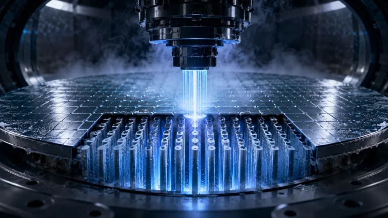
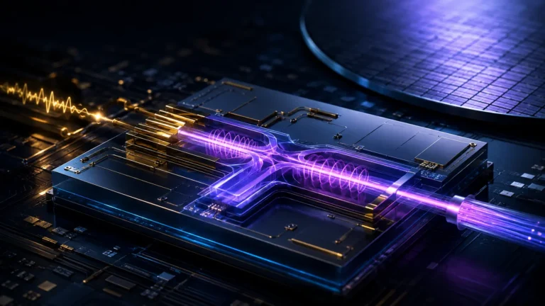
Cryogenic dielectric etching utilizes sub-zero temperatures to alter plasma chemistry, allowing semiconductor manufacturers to drill microscopic, perfectly straight trenches through 400-layer memory chips at unprecedented speeds without the walls caving in.